The Future of ASIC Design: Why Chip Disaggregation Is Redefining Custom Silicon
ElectronicsIntroduction
For decades, application-specific integrated circuits (ASICs) followed a straightforward trajectory. Improvements in semiconductor manufacturing enabled engineers to place more logic on a single piece of silicon, increasing performance while reducing power consumption and manufacturing costs. Monolithic designs became the standard approach for networking equipment, multimedia processors, storage controllers, and countless embedded systems.
That model is gradually reaching its practical limits.
Artificial intelligence, high-performance computing, autonomous systems, advanced networking, and edge computing have introduced workloads that differ dramatically in computational characteristics, memory behavior, latency sensitivity, and power requirements. Optimizing every subsystem within a single monolithic die has become increasingly difficult from both an engineering and an economic perspective.
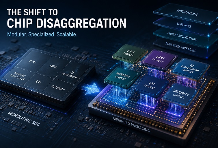
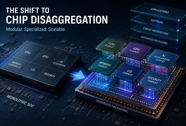
As a result, the semiconductor industry is moving toward a modular design philosophy in which complex processors are assembled from multiple specialized dies rather than manufactured as one large chip.
Chip disaggregation is no longer viewed simply as an advanced packaging technique. It has become a fundamental architectural strategy for building next-generation silicon.
The End of the Monolithic Scaling Era
Traditional ASIC development relied heavily on process node improvements.
Every new manufacturing generation enabled higher transistor density, lower power consumption, and greater computational capability without requiring fundamental architectural changes.
While Moore’s Law continues to deliver improvements, scaling no longer provides the economic advantages it once did.
Leading-edge process nodes require enormous engineering investment, mask costs have risen dramatically, and manufacturing yields decline as die sizes increase.
Large monolithic chips also concentrate risk.
A manufacturing defect affecting any critical region can render an entire die unusable, reducing production yield and increasing overall cost.
As transistor counts continue growing into the tens or even hundreds of billions, these challenges become increasingly significant.
Modern Workloads Demand Specialized Silicon
Artificial intelligence has fundamentally altered semiconductor design priorities.
Unlike conventional embedded applications, AI workloads exhibit widely varying computational characteristics throughout execution.
Some operations are compute intensive, requiring massive parallel arithmetic throughput.
Others are limited primarily by memory bandwidth.
Still others depend on extremely low communication latency between processing elements.
Attempting to optimize every workload using identical hardware inevitably introduces inefficiencies.
Instead, modern accelerator architectures increasingly separate functional responsibilities into dedicated hardware blocks optimized for individual computational tasks.
This philosophy extends beyond AI.
Automotive platforms combine sensor fusion, neural inference, functional safety, networking, and real-time control within the same electronic system.
Telecommunications infrastructure integrates packet processing, encryption, signal processing, and network management.
Industrial automation demands deterministic latency while simultaneously executing sophisticated machine learning algorithms.
Each workload benefits from different silicon optimizations.
From Monolithic Chips to Chiplet Architectures
Rather than integrating every subsystem onto one die, modern semiconductor architectures divide functionality across multiple smaller dies connected through high-bandwidth interconnect technologies.
Each die can be designed, manufactured, and optimized independently before being integrated into a complete package.
This modular approach provides several important advantages.
Compute engines can use the most advanced manufacturing node while analog circuitry remains on mature process technologies better suited for mixed-signal design.
Memory controllers, I/O subsystems, security processors, networking interfaces, and specialized accelerators can evolve independently without requiring complete chip redesigns.
Development teams gain significantly greater architectural flexibility while reducing design complexity.
Instead of treating the processor as a single integrated circuit, engineers increasingly view it as an interconnected system of highly specialized silicon components.
Advanced Packaging Becomes Part of the Architecture
Disaggregation would not be practical without major advances in semiconductor packaging.
Technologies such as 2.5D integration, 3D stacking, silicon interposers, hybrid bonding, wafer-to-wafer assembly, and wafer-to-die bonding now allow multiple dies to communicate with bandwidth approaching that of on-chip connections.
Packaging has therefore evolved from a manufacturing concern into an architectural discipline.
Communication latency, signal integrity, thermal behavior, power delivery, and interconnect density all influence system performance.
Architectural decisions increasingly depend on packaging capabilities just as much as transistor-level implementation.
Successful chip development now requires close collaboration between circuit designers, package engineers, manufacturing specialists, and thermal engineers from the earliest design stages.
Economic Benefits of Disaggregation
One of the strongest motivations behind chiplet architectures is improved manufacturing efficiency.
Smaller dies typically achieve higher fabrication yields because manufacturing defects affect a smaller silicon area.
Rather than discarding an entire processor due to a localized defect, manufacturers lose only the affected chiplet.
Production also becomes more flexible.
Individual chiplets can be reused across multiple products, reducing engineering effort while accelerating new product development.
A common I/O die, for example, may support several generations of compute accelerators.
Similarly, networking, memory interface, and security chiplets can serve multiple processor families with only minor modifications.
This modular reuse significantly lowers long-term development costs.
Verification Becomes More Complex
Although chip disaggregation simplifies certain aspects of design, it introduces new engineering challenges.
Verification no longer focuses solely on individual silicon components.
Engineers must validate complete heterogeneous systems containing multiple dies manufactured using different process nodes and potentially different fabrication technologies.
Inter-chip communication protocols, synchronization behavior, clock distribution, thermal interactions, power sequencing, and fault tolerance all require extensive verification.
Testing complexity also increases substantially.
Each chiplet must be validated independently before packaging, followed by additional testing after final assembly.
System-level reliability depends not only on individual dies but also on the integrity of every interconnect between them.
As semiconductor packages continue growing in complexity, verification increasingly becomes one of the largest contributors to project schedules.
Thermal and Power Optimization
Power distribution has always been a critical aspect of semiconductor engineering.
Disaggregated architectures introduce additional considerations.
Different chiplets generate heat at different rates, creating localized thermal hotspots that influence neighboring components.
Power delivery networks must maintain stable operation across multiple interconnected dies while minimizing electrical noise and voltage fluctuations.
Thermal management therefore becomes a system-wide optimization problem rather than a characteristic of individual chips.
Simulation environments increasingly combine electrical, mechanical, and thermal analysis to evaluate complete package behavior before manufacturing begins.
Software and Hardware Must Evolve Together
Another major shift in ASIC development is the growing dependence between hardware architecture and software optimization.
Modern AI accelerators are often designed alongside compiler infrastructure, runtime libraries, scheduling algorithms, and machine learning frameworks.
Hardware capabilities increasingly reflect expected software execution patterns.
This level of hardware-software co-design encourages modular architectures.
As algorithms evolve, specialized processing elements can be updated independently without redesigning the entire processor.
Chiplet-based systems therefore provide greater flexibility for adapting to rapidly changing software ecosystems.
Reusable IP as a Strategic Asset
Successful modular semiconductor platforms depend heavily on reusable intellectual property.
High-speed interfaces, memory controllers, PCI Express connectivity, Ethernet subsystems, security engines, clock management circuits, and debugging infrastructure represent substantial engineering investments.
Reusing these proven components reduces development risk while shortening verification cycles.
Rather than building every subsystem from scratch, organizations increasingly assemble processors from validated building blocks that have already demonstrated manufacturing reliability.
Reusable IP has become one of the primary enablers of scalable ASIC development.
Ecosystem Collaboration Is Becoming Essential
Few organizations possess expertise across every discipline required for modern semiconductor development.
Advanced node implementation.
Physical design.
Package engineering.
Signal integrity.
Power delivery.
Manufacturing qualification.
Design-for-test.
Functional safety.
Software optimization.
Each discipline requires specialized knowledge and dedicated engineering resources.
Consequently, ASIC development has become increasingly collaborative.
Chip manufacturers, foundries, packaging providers, EDA vendors, IP suppliers, and system integrators now contribute throughout the product lifecycle rather than operating as isolated participants.
The semiconductor ecosystem has shifted from designing individual chips to engineering complete heterogeneous computing platforms.
Looking Ahead
Several industry trends suggest that chip disaggregation will continue expanding over the coming decade.
Artificial intelligence models continue growing in complexity.
Memory bandwidth requirements increase every generation.
Specialized accelerators are becoming more diverse.
Advanced packaging technologies continue improving interconnect density and manufacturing reliability.
Open standards such as Universal Chiplet Interconnect Express (UCIe) are encouraging greater interoperability between chiplets developed by different vendors.
Future semiconductor systems are likely to resemble modular computing platforms assembled from standardized building blocks rather than entirely custom monolithic processors.
This evolution has the potential to reduce development costs while accelerating innovation across multiple application domains.
Conclusion
Chip disaggregation represents more than an incremental improvement in semiconductor packaging. It reflects a broader transformation in how custom silicon is conceived, designed, manufactured, and deployed.
As workloads become increasingly heterogeneous and process technologies grow more expensive, modular architectures offer a practical path toward higher performance, improved manufacturing efficiency, and greater design flexibility.
The transition also changes the nature of ASIC engineering itself. Success increasingly depends on system-level thinking that spans architecture, software, packaging, manufacturing, verification, and thermal design.
The future of custom silicon will not be defined by ever-larger monolithic dies, but by intelligent combinations of specialized chiplets working together as unified computing systems. Organizations capable of mastering this multidisciplinary approach will be best positioned to develop the next generation of high-performance semiconductor platforms.